PN junction diode simulator
Visualize and experiment with depletion region, carrier flow, and energy bands in a PN junction diode using our interactive simulator.
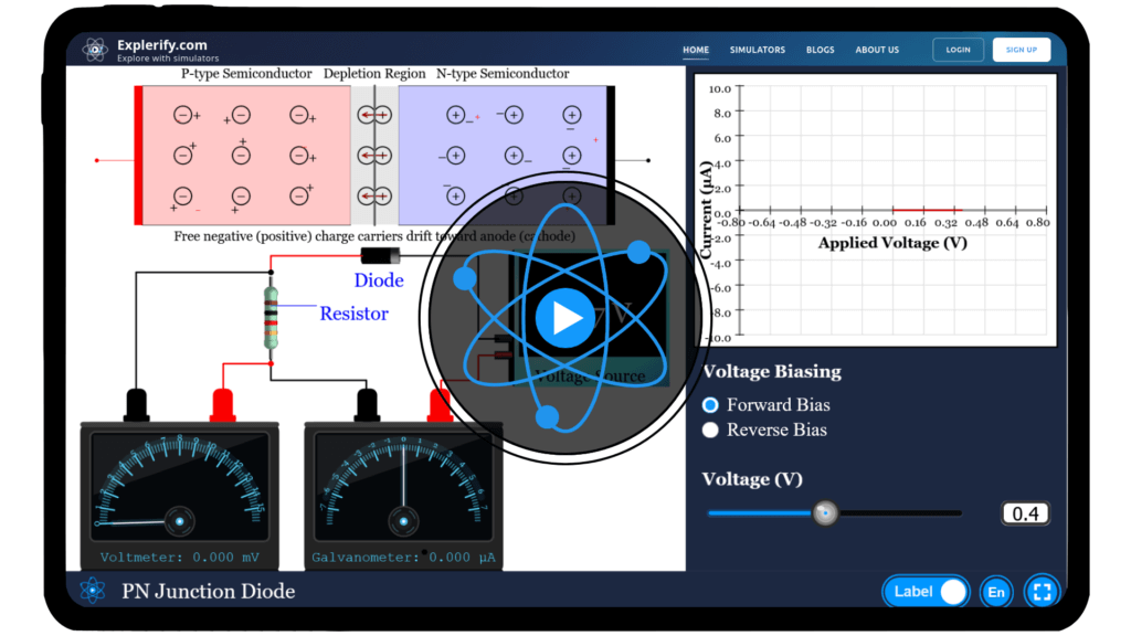
PN junction diode
Ever wondered how electricity flows in the tiny heart of modern electronics? The secret lies in the PN junction diode—a fundamental building block that controls current using the magic of semiconductors. Our PN Junction Diode Simulator brings this microscopic world to life, letting you explore depletion regions, carrier flow, and band bending in both forward and reverse bias. Adjust the voltage, watch the changes unfold, and gain an intuitive grasp of how diodes really work. Dive in and start experimenting now!
\( I = I_s \left( e^{\frac{V}{n V_T}} – 1 \right) \)
Mathematical description
where:
- \( I \) is the diode current
- \( I_s \) is the saturation current
- \( V \) is the voltage across the diode
- \( n \) is the ideality factor
- \( V_T \) thermal voltage (~26 mV at room temperature)
Simulator
Experiment with the controls, vary the applied voltage, and see how it affects the depletion region, carrier flow, and energy bands in a PN junction diode.
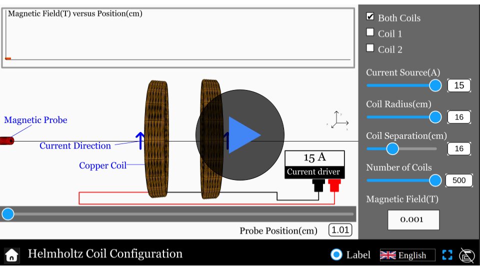
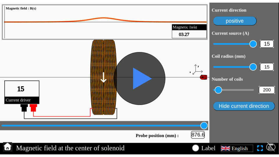
Interactive Physics Simulator – Anti-Helmholtz Coils
🌟 You May Also Like
Suggested experiments and activities based on your progress...
FAQs on PN junction diode
Qus 1. What is a PN junction diode?
A PN junction is formed when a p-type semiconductor and an n-type semiconductor are joined together. At the junction, electrons and holes diffuse, creating a depletion region with an electric field.
Qus 2. What happens at the depletion region of a PN junction?
The depletion region is formed when electrons from the n-side recombine with holes from the p-side. This region has no free charge carriers but contains immobile ions that set up a potential barrier. Applying a forward voltage reduces the barrier, allowing current to flow, while reverse voltage increases the barrier, restricting current.
Qus 3. What is forward bias in a PN junction?
In forward bias, the p-side is connected to the positive terminal and the n-side to the negative terminal of a battery. This reduces the barrier potential, allowing current to flow easily across the junction.
Qus 4. What is reverse bias in a PN junction?
In reverse bias, the p-side is connected to the negative terminal and the n-side to the positive terminal. This increases the barrier width, blocks current flow, and only a tiny leakage current flows.
Qus 5. Why does current flow in forward bias but not in reverse bias?
In forward bias, the applied voltage reduces the depletion barrier, allowing charge carriers to cross the junction. In reverse bias, the barrier widens, blocking carriers and preventing current flow.
Qus 6. What is the VI characteristic of a PN junction?
The VI characteristic shows that in forward bias, the diode conducts beyond a threshold voltage (≈0.7 V for silicon, 0.3 V for germanium). In reverse bias, current is almost zero until breakdown occurs.
Qus 7. What is barrier potential in a PN junction?
The barrier potential is the built-in voltage that opposes further diffusion of charge carriers at the junction. Its typical value is about 0.7 V for silicon and 0.3 V for germanium.
Qus 8. What are the main applications of a PN junction diode?
- Rectification (AC to DC conversion) in power supplies – A PN junction diode allows current to flow in only one direction, converting alternating current into direct current.
- Signal demodulation in communication systems – Diodes detect and separate audio signals from high-frequency carrier waves in radios and communication devices.
- Voltage regulation (Zener diodes) – A Zener diode maintains a stable output voltage by operating in reverse breakdown, protecting circuits from fluctuations.
- Light emission (LEDs) – When forward biased, recombination of electrons and holes in a PN junction releases energy as visible light.
- Photodetection (photodiodes, solar cells) – In reverse bias, PN junctions generate current when exposed to light, converting photons into electrical signals or power.
- Clipping and clamping circuits in signal processing – Diodes shape and modify input waveforms by restricting voltage levels to a set range.
Qus 9. What is breakdown in a PN junction?
When reverse bias voltage becomes very high, the depletion region breaks down, leading to a sudden large current. This is called junction breakdown (Zener or avalanche breakdown depending on the mechanism).
I liked this so much .It was my dream to make a game app on 11 and 12 th science electronics but it’s ok I will give it a five star rating
Hi Keya,
Thank you for your appreciation! We’re really glad you liked Explerify. Keep watching this space- one day we might surprise you with a more gamified experience!